tlc_config.h File Reference
Configuration for the Arduino Tlc5940 library. More...
#include <stdint.h>
#include "pinouts/chip_includes.h"
Go to the source code of this file.
Defines | |
| #define | TLC_BITBANG 1 |
| Bit-bang using any two i/o pins. | |
| #define | TLC_SPI 2 |
| Use the much faster hardware SPI module. | |
| #define | NUM_TLCS 1 |
| Number of TLCs daisy-chained. | |
| #define | DATA_TRANSFER_MODE TLC_SPI |
| Determines how data should be transfered to the TLCs. | |
| #define | TLC_CHANNEL_TYPE uint8_t |
| If more than 16 TLCs are daisy-chained, the channel type has to be uint16_t. | |
| #define | TLC_PWM_PERIOD 8192 |
| Determines how long each PWM period should be, in clocks. | |
| #define | TLC_GSCLK_PERIOD 3 |
| Determines how long each period GSCLK is. | |
| #define | VPRG_ENABLED 0 |
| Enables/disables VPRG (TLC pin 27) functionality. | |
| #define | XERR_ENABLED 0 |
Enables/disables XERR (TLC pin 16) functionality to check for shorted/broken LEDs
| |
| #define | VPRG_PIN DEFAULT_VPRG_PIN |
| VPRG (TLC pin 27). | |
| #define | VPRG_PORT DEFAULT_VPRG_PORT |
| #define | VPRG_DDR DEFAULT_VPRG_DDR |
| #define | XERR_PIN DEFAULT_XERR_PIN |
| XERR (TLC pin 16). | |
| #define | XERR_PORT DEFAULT_XERR_PORT |
| #define | XERR_DDR DEFAULT_XERR_DDR |
| #define | XERR_PINS DEFAULT_XERR_PINS |
| #define | SIN_PIN TLC_MOSI_PIN |
| SIN (TLC pin 26). | |
| #define | SIN_PORT TLC_MOSI_PORT |
| #define | SIN_DDR TLC_MOSI_DDR |
| #define | SCLK_PIN TLC_SCK_PIN |
| SCLK (TLC pin 25). | |
| #define | SCLK_PORT TLC_SCK_PORT |
| #define | SCLK_DDR TLC_SCK_DDR |
| #define | GS_DUO(a, b) ((a) >> 4), ((a) << 4) | ((b) >> 8), (b) |
| Arranges 2 grayscale values (0 - 4095) in the packed array format (3 bytes). | |
| #define | DC_QUARTET(a, b, c, d) |
| Arranges 4 dot correction values (0 - 63) in the packed array format. | |
Detailed Description
Configuration for the Arduino Tlc5940 library.After making changes to this file, delete Tlc5940.o in this folder so the changes are applied.
A summary of all the options:
- Number of TLCs daisy-chained: NUM_TLCS (default 1)
- Enable/Disable VPRG functionality: VPRG_ENABLED (default 0)
- Enable/Disable XERR functionality: XERR_ENABLED (default 0)
- Should the library use bit-banging (any pins) or hardware SPI (faster): DATA_TRANSFER_MODE (default TLC_SPI)
- Which pins to use for bit-banging: SIN_PIN, SIN_PORT, SIN_DDR and SCLK_PIN, SCLK_PORT, SCLK_DDR
- The PWM period: TLC_PWM_PERIOD (be sure to change TLC_GSCLK_PERIOD accordingly!)
How to change the pin mapping:
- Arduino digital pin 0-7 = PORTD, PD0-7
- Arduino digital pin 8-13 = PORTB, PB0-5
- Arduino analog pin 0-5 = PORTC, PC0-5
Define Documentation
| #define DATA_TRANSFER_MODE TLC_SPI |
Determines how data should be transfered to the TLCs.
Bit-banging can use any two i/o pins, but the hardware SPI is faster.
- Bit-Bang = TLC_BITBANG
- Hardware SPI = TLC_SPI (default)
| #define DC_QUARTET | ( | a, | |||
| b, | |||||
| c, | |||||
| d | ) |
Value:
((a) << 2) | ((b) >> 4), \
                                 ((b) << 4) | ((c) >> 2), \
                                 ((c) << 6) | (d)
- See also:
- setDCtoProgmemArray
| #define GS_DUO | ( | a, | |||
| b | ) | ((a) >> 4), ((a) << 4) | ((b) >> 8), (b) |
Arranges 2 grayscale values (0 - 4095) in the packed array format (3 bytes).
This is for array initializers only: the output is three comma seperated 8-bit values.
| #define NUM_TLCS 1 |
Number of TLCs daisy-chained.
To daisy-chain, attach the SOUT (TLC pin 17) of the first TLC to the SIN (TLC pin 26) of the next. The rest of the pins are attached normally.
- Note:
- Each TLC needs it's own IREF resistor
| #define TLC_CHANNEL_TYPE uint8_t |
If more than 16 TLCs are daisy-chained, the channel type has to be uint16_t.
Default is uint8_t, which supports up to 16 TLCs.
| #define TLC_GSCLK_PERIOD 3 |
Determines how long each period GSCLK is.
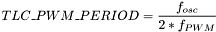
This is related to TLC_PWM_PERIOD: 
- Note:
- Default is 3
| #define TLC_PWM_PERIOD 8192 |
Determines how long each PWM period should be, in clocks.
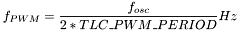
 This is related to TLC_GSCLK_PERIOD:
- Note:
- The default of 8192 means the PWM frequency is 976.5625Hz
| #define VPRG_ENABLED 0 |
Enables/disables VPRG (TLC pin 27) functionality.
If you need to set dot correction data, this needs to be enabled.
- 0 VPRG is not connected. TLC pin 27 must be grounded! (default)
- 1 VPRG is connected
- Note:
- VPRG to GND inputs grayscale data, VPRG to Vcc inputs dot-correction data
| #define XERR_ENABLED 0 |
Enables/disables XERR (TLC pin 16) functionality to check for shorted/broken LEDs
- 0 XERR is not connected (default)
- 1 XERR is connected.
- Note:
- XERR is active low
